CEA-LITEN
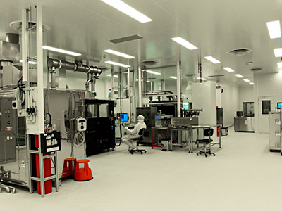
PICTIC is a technological platform dedicated to electronics and printed sensors. It is located at the CEA-Liten in Grenoble, an European institute dedicated to new energy technologies and materials. PICTIC offers industry development and prototyping services along the length of the printed electronics value chain: materials, printing processes, components and integration into the product. The platform is supported by the Auvergne Rhône-Alpes region and FEDER funds.
40 research workers and technicians
€8 M
Portfolio of 50 patents
600m² of white rooms
Industrial partnerships:
Numerous industrial partnerships (bilateral agreements, funded projects) with material& equipment or component manufacturers, plasturgists, end-users(mobility, security, sport, health..)
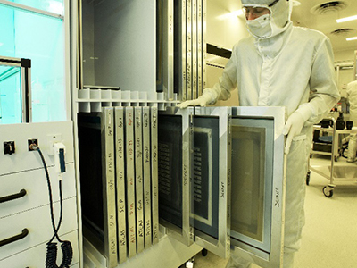
Printing equipments, unique in Europe
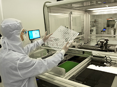
PICTIC covers all processes involved in the creation of flexible electronic components:
Ink jet and ultrasonic spray
Rotogravure and flexographics,
Slot-die coating
Screen printing
High rate laser ablation
Laminating, electric inter-connections
Characterisation and ageing of components.
All processes are sheet by sheet and use various types of substrates (plastic, paper, metal...) at a standard size of 32 x 38 cm. A complementary Printed Photovoltaic Platform in the National Solar Energy Institute (INES) gathers a set of pre-industrial equipments in Sheet- To-Sheet format (30x30 cm inkjet printers) and Roll-to-Roll format (500 mm width).
Components and systems
CEA Liten develops logic functions, displays and printed sensors on large size, flexible substrates:
- Passive components: resistors, aerials, RLCs.
- Logic functions: transistors for circuits (AD converters, amplification) and address matrix, memories.
- Sensors and sensor matrix: temperature, pressures, photodiodes, biochemical...
- Haptic functions
- Capacitive sensors
- Photovoltaic cells
- Piezo active devices
- Plastronics (in collaboration with IPC:Innovation Plasturgie Composite technical center)
Services to industry
CEA Liten offers a wide range of services for the development of printed electronic functions:
- Qualification of materials and substrates, ink formulation.
- Study of new components and circuits.
- Development of component manufacturing processes.
- Modelling, design, characterisation and ageing of components and circuits.
- Interconnection and integration of components into products.
- Prototyping in short runs and transfer of processes to industrial use.
Partnerships
We work with industrial partners along the length of the printed electronics value chain. As an example, in partnership with leading chemical company, we are working on the development of new inks and their integration into sensors, actuators and memories.
We are also working with leading paper firm, on the development of new cellulose substrates and their applications in printed electronics.
Emmanuelle VÉRAN
Responsable partenariats industriels
Tél : +33 (0)4 38 78 29 49
Emmanuelle.veran@cea.fr
Christophe SERBUTOVIEZ
Responsable technique de la plate-forme
Tél : +33 (0)4 38 78 23 01
christophe.serbutoviez@cea.fr
Site internet
https://liten.cea.fr/cea-tech/liten/english/


