SEMILAB
Process control equipment can be implemented in-line in the production flow, offline with appropriate sampling, or even integrated into manufacturing equipment, such as roll-to-roll coaters.
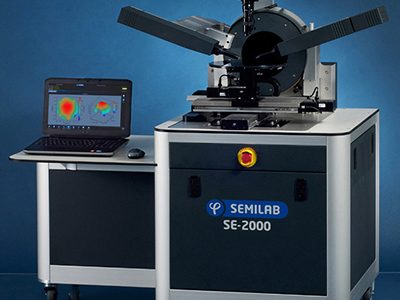
SEMILAB design, produce and sell metrology equipment for the characterization of semiconductor, photovoltaic, display and printed electronics materials, for monitoring the manufacturing process, and also for R&D purposes in these areas.
We offer a variety of measurement techniques; many of which are non-contact and non-destructive. These technologies can be flexibly integrated in different platforms, ranging from simple handheld devices and table-top systems with high resolution mapping capability, to fully automated stand-alone production control tools
for mid-range and high-level fab lines.
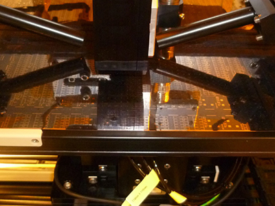
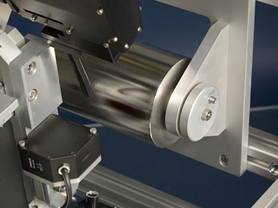
We also offer in-line measurements for various production lines like OPV on roll to roll coaters.
Our strategy is to continuously improve and evolve our products to meet new challenges in applications, and to offer flexible solutions for our customers’ needs with high-value added solutions. We participate in various international R&D projects and European contracts.
In addition we carry out this work in a responsible way; providing benefits to employees, research and support important cases such as scientific education.
Optical characterization
SEMILAB provides equipment for complete characterization for thin film layers, such as those used in printed and organic devices including OPV and OLED multilayers.
We offer a wide range of metrology, includingspectroscopic ellipsometry, reflectometry, transmission, photoluminescence, imaging reflectometry and white light interferometry, which enable complete control of all optical properties of such layers.
Electrical characterization
Depending on specific requirements, contact or non-contact techniques could be chosen from the SEMILAB product portfolio to measure electrical film properties.
These may include resistivity and sheet resistance (by 4 Point Probe, or non-contact eddy current), lifetime (by μ-PCR), etc. in thin metallic, organic semiconductor, and of course the transparent conductive electrode layers.
Platforms
SEMILAB provides R&D type tools for small size samples, intermediate platforms (up to 450x 450 mm), and large production scale platforms for glass, or sheet to sheet on flexible substrate process development and control. Real time in-line control solutions are also possible for belt type conveyers, or on continuous Roll to Roll type processing equipment, providing fast and accurate real time measurements.
SEMILAB Semiconductor Physics
Laboratory Co. Ltd.
Prielle Kornélia str. 2.
H-1117
BUDAPEST - Hongrie
Tél : +36 (0)1 505 4690
Fax : +36 (0)1 505 4695
Contact
Information
semilab@semilab.com
Contact ventes
sales.support@semilab.com
Contact technique
technical.support@semilab.com
Contacts France
Nicolas LAURENT
Tél : +33 (0)6 75 06 70 40
nicolas.laurent@semilab.com
Christophe DEFRANOUX
Site internet
https://www.semilab.hu/